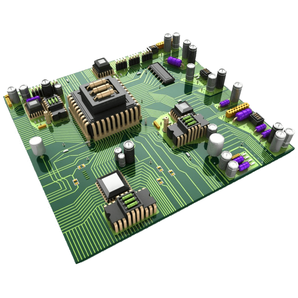
At PCB Advance, We provides offshore front-end engineering and test services & CAM projects (PCB Designing) for Printed Circuit Board Industry. we continue to improve efficiency and productivity while focusing on continuous improvement of our quality & services to surpass our customer’s expectations. We can use any information you have and create a fully functional data for you to manufacture a board. We can accept various file formats with our state-of-the-art CAM software.We have ability to work on Software like Ucamco UCAM, Genesis 2000, CAM 350, Speed Stack Polar software etc…
Experience to handled customers in many different fields of the electronics industry, including Automotive, Aerospace, Defense, Consumer Electronics, Telecoms, Medical, Space, Marine, and Oil.

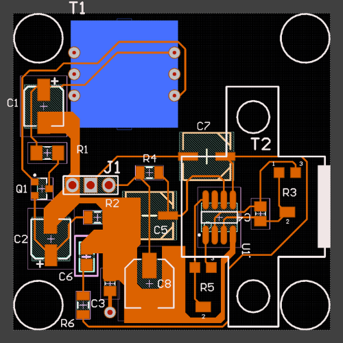
- Full-fledged and dedicated CAM facility for Gerber data post-processing (Pre-Manufacturing)
- 24/7 service availability to meet global customer demands
- Advanced software, hardware, and communication infrastructure
- Netlist analysis and optimization services
- Editing, optimization, and rout retention
- Step and repeat with break-away tabs
- Support for slots, scoring, V-cuts, and routing
- Tear dropping implementation
- Multi-circuit panelization capabilities
- Test coupon creation
- Re-tooling existing parts without affecting ongoing production
- Extensive DFM actions across various layers, including Signal, Solder Mask, and Silk Screen, to ensure high productivity.
- Thorough analysis of Gerber data along with Fab drawing for accuracy.
- Verification of board outline dimensions, hole size, hole count, and tolerances.
- Review of stack-up information, finish type, and board thickness specifications.
- Special attention to unique text and logo requirements.
- Complete panelization for single-sided, double-sided, and multi-layer boards.
- Generation of drill and routing programs from AutoCAD/DXF or Gerber files.
- Supports data in Gerber, RS-274X, DXF, PDF, HPGL, AutoCAD, ASCII, or NC Drill formats.
- Detection of missing holes, extra holes, or closely spaced holes.
- Identification of touching or duplicate holes.
- Verification for the second drill option.
- Ensuring minimum spacing between two conductors.
- Adherence to minimum track width specifications.
- Validation of the minimum annular ring size.
- Drill/rout to conductor spacing checks.
- Detection of sliver issues.
- Thermal air gap and spoke width verification.
- Drill to copper plane spacing checks.
- Ensuring plane shearing line width accuracy.
- Mask annular ring validation for copper pads.
- Verification of exposed trace areas.
- Mask to copper spacing checks.
- Ensuring proper legend width.
- Conversion of draws to flash for efficiency.
- Ensuring accurate pad registration.
- Removal of non-functional pads (NFP).
- Elimination of redundant pads and lines.
- Unification of lines for cleaner designs.
- Correction of self-intersecting polygons through countrization.
- Detection and correction of sliver in acute angles.
- Verification of SMD attributes for proper placement.
- Detection and validation of legends for clarity
- Power ground optimization.
- Signal layer optimization.
- Teardrop creation.
- Solder mask optimization.
- Legend overlap.
- Copper Balancing.
- Etch Compensation
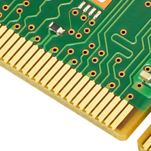
- Support for Gold Finger application for edge connectors.
- Controlled impedance for high-frequency circuit performance.
- Via-plug, peelable mask, and carbon ink options for specialized designs.
- Flip flop panelization technique for efficient board layout.
- Flat pad implementation for enhanced solderability.
- Flex and Flex-Rigid board support for dynamic and complex applications
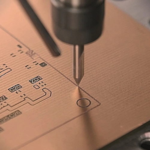
- Generation of NC drill and rout programs for automated machining.
- Development of rout programs for plated edges, executed after drilling and before etching.
- Creation of a second stage drill program for precise hole placement.
- Implementation of counterbore and countersink features for smooth finishes.
- Design of panels with tab routs and breakout pips for easy handling.
- Utilization of peck drilling (G85) for effective material removal.
- Control depth rout programming for consistent routing depths.
- Scoring program development for clean and accurate board outlines.
- Tool path generation for optimized machining efficiency.
- Cover layer and stiffener program creation for enhanced board stability
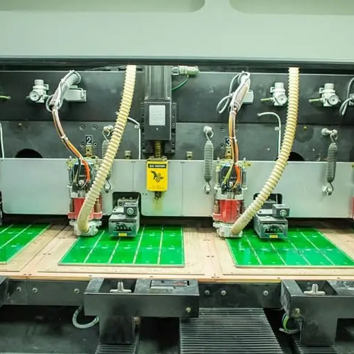
- Step and repeat of boards on large panels for efficient production.
- Implementation of venting patterns for optimal airflow.
- Inclusion of tooling holes, registration targets, and punch targets for precision.
- Creation of coupons for controlled impedance projects.
- Compensation strategies for lamination shrinkage to maintain dimensional accuracy

- Scripting: Customers can obtain the necessary scripts tailored to their production needs within the CAM tool system.
- Hyper Tooling: A Java-based program designed to automate routine tasks in tooling, enhancing efficiency.
- Tooling: Managed by a skilled team of engineers, this process involves handling design data from initial input, performing cleanup, conducting DRC/DFM and board edits, and completing all necessary tasks up to output